
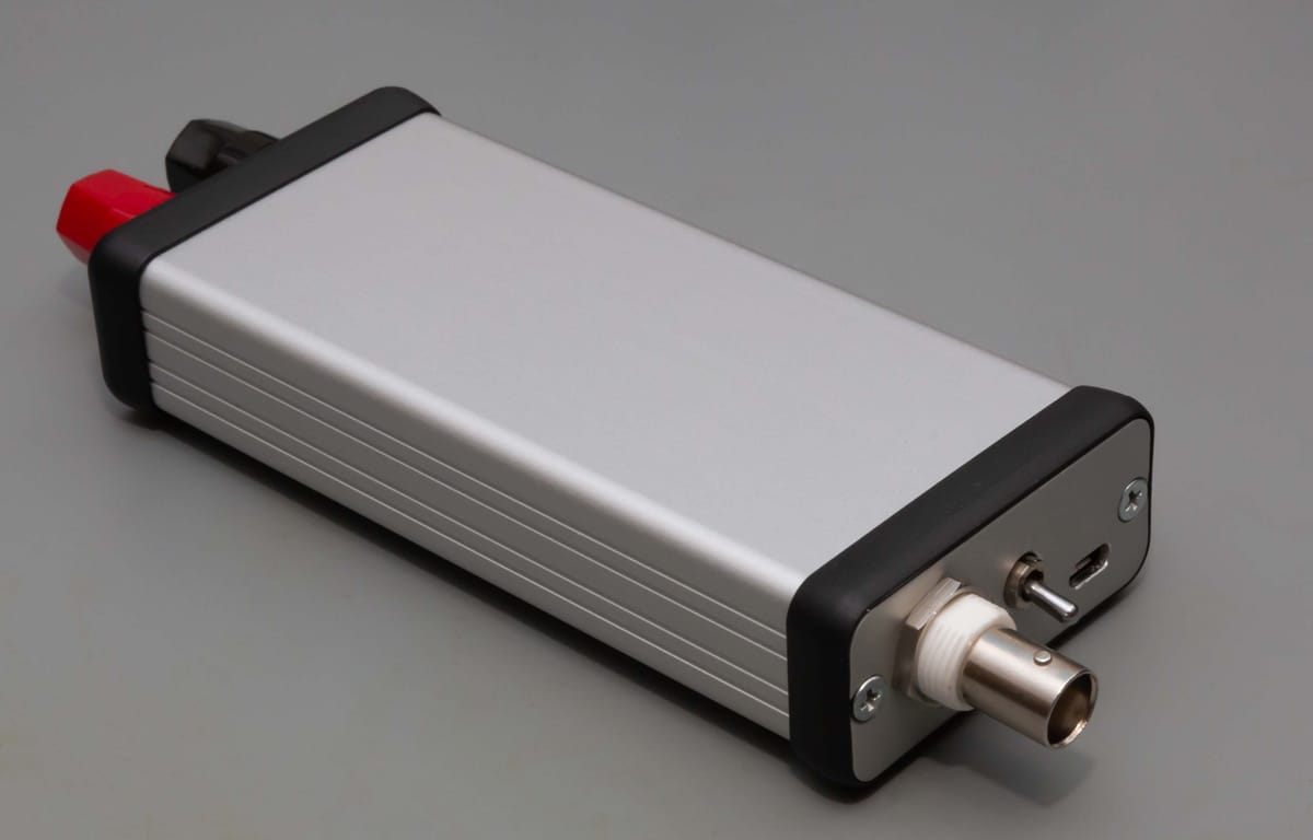
Differential Current Probe
A USB-powered 20A shunt ammeter with 1MHz bandwidth.
I recently found myself in need of a reliable way to measure AC + DC current in the tens of Amps, and wanted to do so at frequencies up to around 1MHz to catch some fast transient behavior of a programmable DC load in my lab. There are a number of existing probe solutions for oscilloscopes that solve this problem, but many of the high quality options (these, for example) significantly exceed my budget. The less expensive probe options (for example Hantek's line of clamp current probes) have some significant limitations in terms of frequency range and output noise. Since I can't justify the expense of a "real" current probe, and am not satisfied with the performance of the less expensive options, I decided to build my own current probe.
Theory
Commercial probe solutions seem to use a fluxgate sensing approach, where an external drive coil closes a magnetic feedback loop including a hall-effect type sensor. This approach can give a frequency response down to DC with good performance, while still providing the advantage of a non-contact current measurement inherent to magnetic current sensing. Unfortunately, commercial products seem to target lower-frequency operation than I’m interested in – I’d like a solution to measure currents up to 1MHz or so, while the commercial fluxgate options seem to target frequencies up into the hundreds of kilohertz. Designing magnetics for a non-invasive magnetic current probe was also not a challenge I wanted to take on.
Due to the complexity of implementing a magnetic current probe at the bandwidth I’m interested in, I decided to go with a simpler shunt resistor design instead.
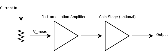
A resistive shunt is not fundamentally a difficult design. The current to be measured is run through a resistor, and the resulting voltage drop is measured using a differential amplifier. The signal may need additional gain (if not provided by the differential amplifier) to scale it appropriately and improve signal to noise ratio. At the end of the chain, the signal is applied to an oscilloscope or DMM to display the measurement.
Resistive measurement does have some shortcomings. A shunt resistor will develop a burden voltage corresponding to the I*R drop across it. Fortunately, for my application, a burden voltage of a few hundred millivolts isn’t a significant issue, and simply selecting a low-valued shunt resistor should be sufficient to minimize the problem.
Another drawback to the resistive shunt is isolation. With a magnetic current sensor, the measurement circuitry is inherently isolated from the circuit under test. With a resistive shunt, this is no longer the case. For low-side current measurements (measurements made in the ground leg of a circuit), this may not be an issue, but high-side measurements can become a challenge.
If, for example, you wanted to measure the current draw out of a 370V power factor correction circuit, the differential amplifier in your resistive shunt probe would have to tolerate a 370V common mode voltage riding on top of the millivolt-scale signal of your current waveform. Fortunately, for moderate common-mode voltages (in my case, 50V max) this challenge is far from insurmountable with a little analog trickery.
Goals
I'd like to end up with a resistive current probe that can do the following:
- Measure bidirectional current in the range of ±20A
- Provide a usable bandwidth (-3dB point) of 1MHz or more, giving enough bandwidth to capture fast or unusual transients
- Tolerate an input common-mode range up to around ±50V
- Be powered via a micro-USB connector - I have a number of instruments with USB ports I can use, or can power the probe from a power bank if necessary.
- Provide output via a standard 50-ohm BNC connector.
- Provide input connection options for binding posts and banana jacks.
- Fit inside a nice box.
Simulation
Since almost all of the design decisions are driven by the shunt resistor itself, I chose values for that component first. To achieve a usable current range of ±20A, I selected a 10mΩ shunt resistor. This will produce a burden voltage of ±200mV at the extreme ends of my measurement range, which is low enough to not adversely impact my typical use cases. A 10mΩ shunt at 20A will dissipate 4W of power. I selected a Vishay Dale WSHP2818R0100FEA which is rated for 10W, giving plenty of headroom for this application.
I gave some thought next to power supplies. For initial testing of the Rev A design, I used ±9V supplies from a pair of 9V batteries. For Rev B, I decided to power the op amps from ±10V supplies, though this could be increased if needed. For all simulations described here, ±10V supplies are assumed.
The first challenge in this design is the required common-mode range. Combined with the 1MHz desired bandwidth, this rules out using a commodity instrumentation amplifier - most have common mode voltage limitations significantly below my ±50V range requirement.
Focusing on the common mode requirement first, I started looking at commercial instrumentation amplifiers for inspiration. TI's INA149 advertises a ±275V common mode range, as well as decent DC specifications, but doesn't quite reach the bandwidth I'm looking for. My plan is to use the circuit topology from the INA149 and build a discrete implementation using an op amp instead.
The INA149's clever trick is to add an additional resistor to the inverting input of the op amp inside it. This serves to provide an additional voltage divider effect at this node, effectively reducing the common-mode voltage seen at the op amp's input.
Building this design using discrete resistors does incur a penalty to common-mode rejection, since matching between the resistors and the resistor ratios won't be nearly as good as is possible when doing an IC layout in silicon. That said, resistor matching between parts from the same reel typically significantly exceed the resistor tolerance itself - I've seen matching as good as 10x better than the listed tolerance - so performance shouldn't be too badly impacted.
With the instrumentation amplifier topology chosen, I moved on to selecting an op amp. I decided to evaluate two different options here. First up is the Texas Instruments OPA192, chosen because it has a good combination of low noise and good DC precision, and because it has become my go-to 36V precision op amp. As an upgrade pick, I chose the OPA828 which, while pricy ($7.54 each!) does offer excellent noise, offset, and bandwidth. Schematics were identical between the OPA192 and OPA828 designs.
I suspect that the main limitation in the bandwidth of the INA149 arises due to the RC low pass filter formed by the input resistance (380kΩ) and the input capacitance of the amplifier. Since I'm targeting a lower common-mode range, I opted to reduce the input resistors to 100kΩ, while keeping the 20kΩ value for the input dividers.
With a basic design in mind, I built up a test fixture for the instrumentation amplifier front end as shown:
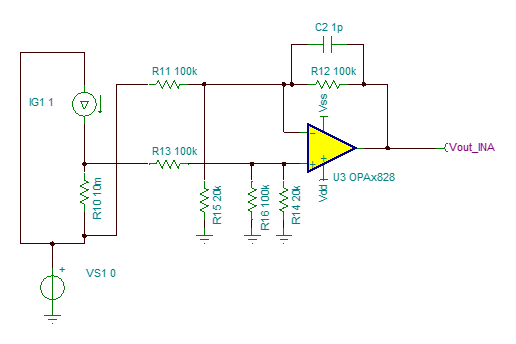
This test circuit includes the 10mΩ shunt, a current source to simulate my input current, and voltage source Vcm which allows me to sweep the circuit over common mode voltage to test CMRR. Simulations of this circuit looked promising, with good DC CMRR (1.2µV over a ±36V common mode range), a -3dB frequency response of 1.2MHz, and total noise of 156µVRMS over that bandwidth when simulated with an OPA192 macromodel. Swapping to the OPA828 maintained good DC performance while increasing the -3dB frequency to almost 2MHz, with an increase to 211µVRMS total noise over the 2MHz bandwidth.
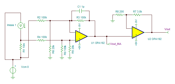
With that positive result, I went on to design my gain stage. Ideally, it would be best to include the gain in the instrumentation stage. However, to do so would require 2MΩ resistors at R3 and R9, which would significantly cut bandwidth and increase noise. Smaller resistor values could be used here if R2, R4, R6, and R9 were also decreased, but this would increase the current (and power dissipation) in these resistors due to any common mode voltage present.
Instead, I opted to add a simple noninverting gain stage following the instrumentation amplifier front-end as shown.
I ran a simulated DC sweep of currents in the ±20A range for this circuit and, to look at overall output error, plotted \( I_{err} = 5*V_{out} - I_{in} \). This should give an indication of the input-referred overall deviation of the probe output from the desired transfer function.
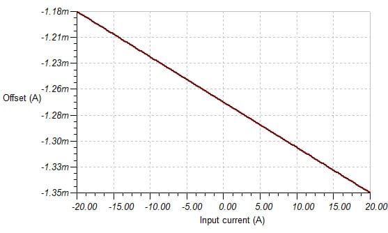
This looks promising. With ideal resistors (perfect matching), error in the output is on the order of mA at the input - good enough for my needs.
Simulating the bandwidth for the complete design, I found that the OPA192 design had a -3dB bandwidth of around 500kHz, which was about half of what I wanted. While it's possible that this could be improved with different compensation, I opted to continue my experiments with the OPA828. The overall frequency response for the OPA828 design is shown below:
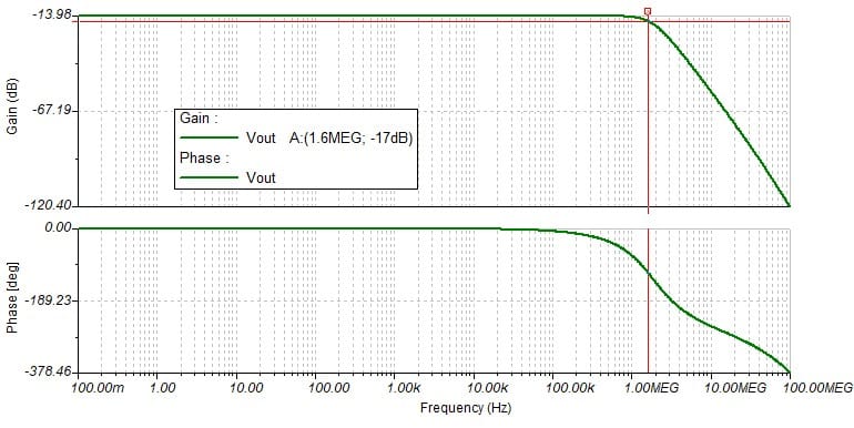
The frequency response is flat out to the 1.6MHz -3dB point with no significant peaking. The phase response of this design looks relatively benign as well, with no sudden phase shifts that might indicate lurking stability issues. Simulated total noise across the full 1.6MHz bandwidth for the OPA828 design was ~3.7mVRMS, corresponding to ~18.5mARMS of apparent noise at the input.
One shortfall in the design is the common mode ran. I originally hoped for a ±50V common mode range. Unfortunately, with ±10V supplies, this isn't possible - simulated common-mode range only extends from -50V to +45V.

While I don't anticipate the reduced common mode range being an issue for my application, it can be improved by increasing the supply voltage to ±11V if necessary. Even with the ±10V supplies, no damage should occur to the op amp at a 50V common mode condition.
Schematic
With encouraging results from simulation, I went ahead and implemented the design in Altium Designer:
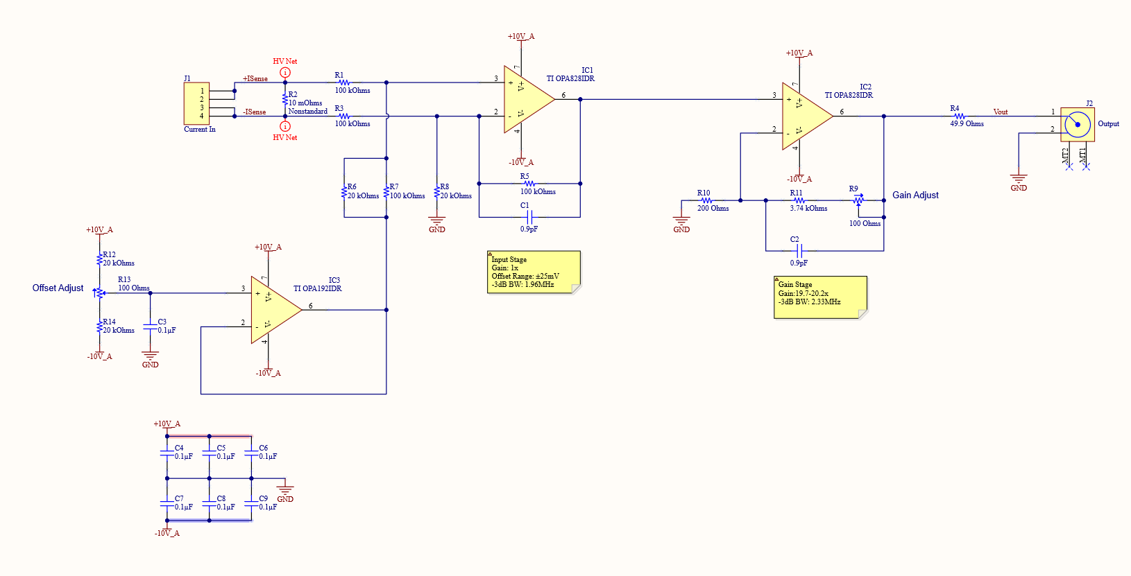
A couple of changes were made to the original design. First, Gain and Offset calibration trimpots were provided to help provide a calibration mechanism. Adjustment ranges for these two controls was chosen to offset the expected worst-case shifts of resistor tolerances in the circuit. Second, 49.9 ohm resistor R4 was added in series with the probe output. This resistor serves two purposes - it provides a source series termination, which is likely unnecessary for the frequency of interest of this design, but it also provides a resistance to isolate IC2's output from the capacitance of the cable, helping to eliminate stability problems due to the cable capacitance.
To help scope design rules, I went ahead and put my two sense lines into a HV net class - I plan on using that net class for clearance and creepage rules, though at 50V the risk is relatively low.
Just in case I encounter unexpected stability issues in the finished design, I've included placeholder capacitor across both feedback resistors.
The power supply design was up next:
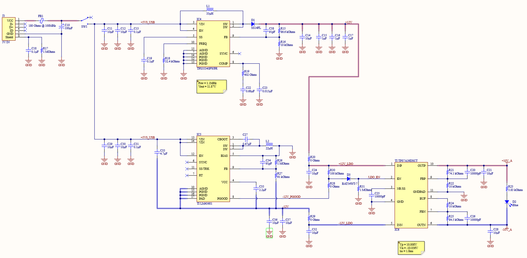
One of my design goals here was for this circuit to be powered from a standard micro-USB cable. The power supply design I settled on is as follows. 5V power is provided from micro-USB connector J5, and is filtered by a ferrite bead and 100µF capacitor C10. When switch SW1 is closed, the 5V supply is provided to IC4, a TPS55340 boost converter, and IC4, an LM43610 configured as an inverting boost converter, which produce ±12V intermediate supply rails. These rails then feed IC6, a TPS7A3901 positive and negative LDO, which in turn produces the ±10V rails that feed the analog circuitry. An LED, D2, provides a visual indication when the ±10V supplies are powered.
Since this design is intended to be powered from a standard USB port, the current draw on the 5V rail needs to remain below 500mA.
Quiescent current consumption for the OPA828 is ~8mA at most, while the OPA192's max is ~1.5mA. This means that the quiescent load on the ±12V rails will be 17.5mA. Assuming an 80% efficiency in the switching supplies, this means the overall quiescent current on the 5V rail will be \(2 * \frac{0.0175 * 12}{0.8 * 5}\), or 105mA.
Worst-case power consumption would occur if the OPA828 output were shorted. In this case, the output current will be limited by the OPA828's current limit of 50mA. It's important to note that this current can only ever be drawn from one supply at a time, so a shorted-output condition would increase 5V supply current by \( \frac{0.05 * 12}{0.8 * 5}\) or 150mA, resulting in a total 5V supply current of 255mA - around half of the 500mA maximum.
Designs for the TPS55340 and LM43610 were provided by TI's Webench tool. I've had good experiences using Webench for applications like this, and it's certainly simpler than working through the datasheet calculations for the switching supply designs.
Another power supply option would have been to use modules, like Analog Devices excellent µModule switching suppplies or TI's Simple Switcher line, but for a design this simple the cost of switching modules would have dominated the overall solution cost, and with little benefit over the discrete implementations used.
Layout
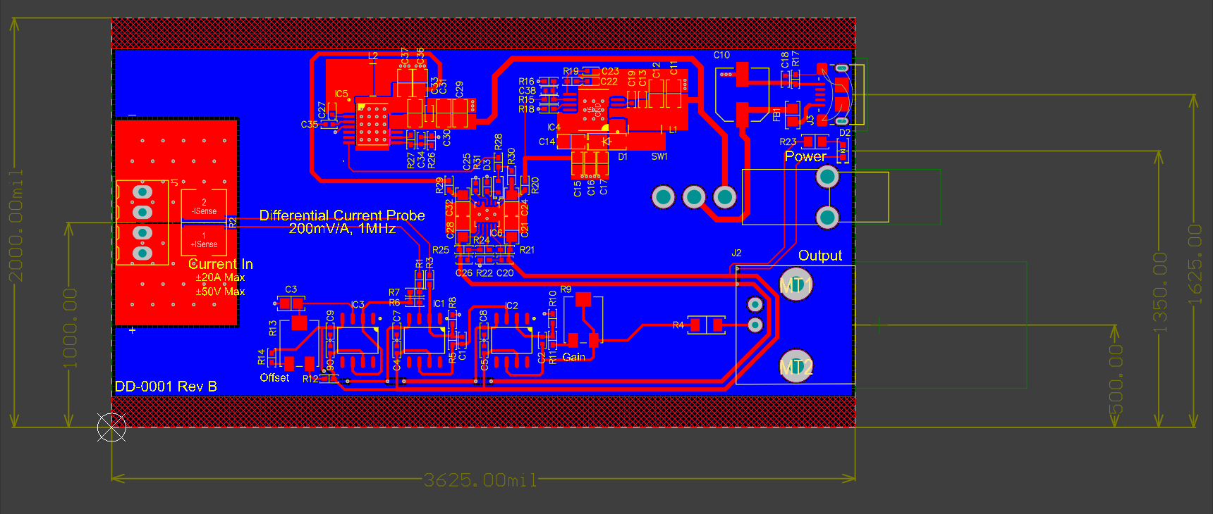
The PCB dimensions here were driven largely by my planned enclosure, a Hammond 1455C1201, which dictated a 2" PCB width (vertical axis). Length was determined by measuring the space required for the terminals of my output binding posts. I set aside keepout areas at the top and bottom of the board to prevent copper from extending into the slots of the Hammond enclosure and minimize the possibility of shorts developing over time if the soldermask was worn through in those aread.
With my dimensions constrained, I began my layout by placing the connectors along the left and right board edges, since these parts were constrained by the finger clearance required to access them and clearance they required to the walls of the enclosure. With these placed, I moved on to the switching supplies and associated components, paying attention to the placement so as to minimize loop areas around the switch nodes. Once the two switching supplies were placed, I could move them slightly to better optimize the placement of the LDO near the center. With the power supplies complete, the analog signal chain was placed and routed next along the bottom edge of the board.
The current input is provided through substantial polygon pours on both the top and bottom of the board, stitched together with vias. Small polygon cutouts were used to create better Kelvin connections to the shunt resistor. While the effect of this design decision is likely to be minimal, it should theoretically result in a slight increase in accuracy.
I had initially considered using a 4-layer stackup for this design, but after some finagling, was able to reduce the layer count to 2 layers with a layout I was still satisfied with. The bottom layer was set aside as much as possible as a solid ground plane, with only small jumpers routed on it in a few places. This should help keep loop areas small and minimize potential noise coupling into the board.
Construction
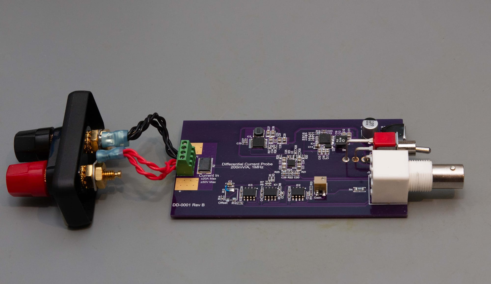
Once the design was passing DRC, I exported Gerber files and sent them to OSH Park for fabrication. For this build, I didn't opt to buy a stencil, and instead used a small applicator needle to apply solder paste to the pads on the board, manually placed my components, and used a combination of hotplate preheat and hot air to reflow the board. A few problem spots where excessive solder paste had been applied were manually reworked. For designs like this, I prefer to use a water-soluble flux. I do two assembly passes. The first pass includes all components that can tolerate an ultrasonic cleaning - switches and relays can be damaged in an ultrasonic cleaner, so they get installed later. After the first assembly, the boards are run through an ultrasonic cleaner filled with distilled water to remove the flux residue. Once the boards are clean and dry, I install any components that wouldn't tolerate the cleaner (switches and potentiometers in this case) and thoroughly clean the affected areas by hand with more distilled water.
Using the 3D models from Altium and Hammond's models for the enclosure, I modeled the assembled probe in Fusion 360. This allowed me to project features from my design, including the connector and switch locations, onto the enclosure model. With the geometry projected, I was able to create prints documenting front-panel hole and slot locations.
Prints in hand, I then machined these on my mill. Unfortunately, I don't have pictures of this process (maybe next time). The setups and milling were all very basic drilling and slotting operations.
Testing
My initial testing focused on the on board power supplies. I initially removed R20 and R29, disconnecting the LDO and op amps from the switching supplies. I provided A 5V supply from my trusty HP E3631A bench power supply (current limited to 200mA just in case), flipped the power switch, and checked voltages at the outputs of both switchers. Once satisfied that both were in-spec, I powered down, replaced R20 and R29, and powered back up.